Question 3 (option)
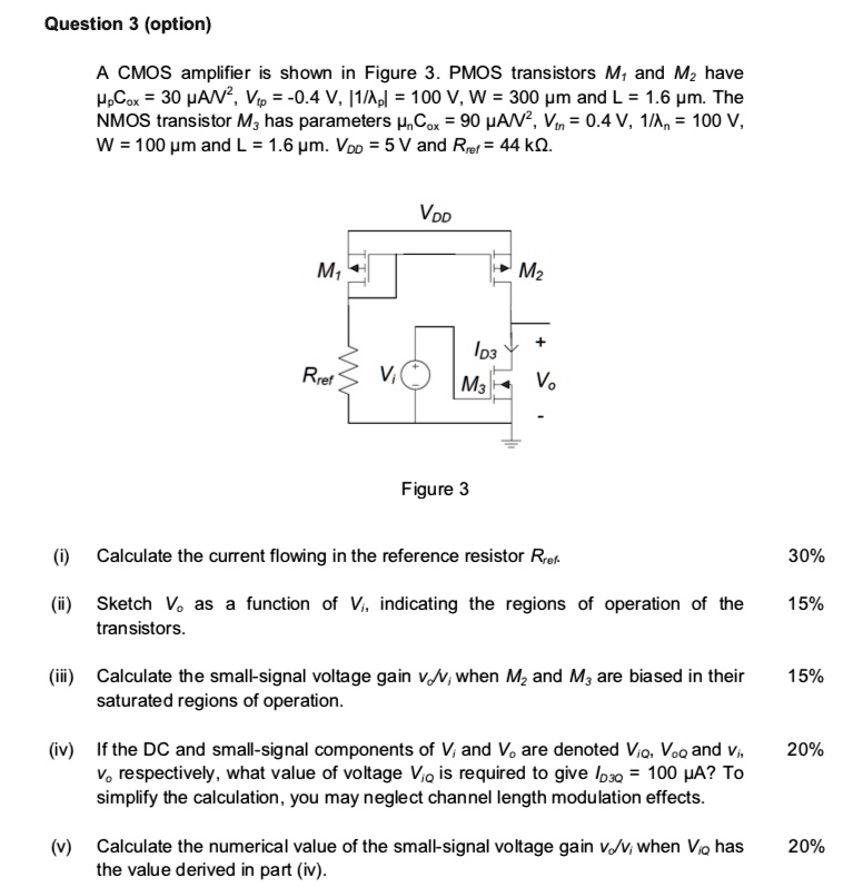
A CMOS amplifier is shown in Figure 3. PMOS transistors $M_1$ and $M_2$ have
$\mu_p C_{ox} = 30 \mu A/V^2$, $V_{tp} = -0.4 \ V$, $1/\lambda_p = 100 \ V$, $W = 300 \mu m$ and $L = 1.6 \mu m$. The
NMOS transistor $M_3$ has parameters $\mu_n C_{ox} = 90 \mu A/V^2$, $V_{tn} = 0.4 \ V$, $1/\lambda_n = 100 \ V$,
$W = 100 \mu m$ and $L = 1.6 \mu m$. $V_{DD} = 5 \ V$ and $R_{ref} = 44 k\Omega$.
(i) Calculate the current flowing in the reference resistor $R_{ref}$.
(ii) Sketch $V_o$ as a function of $V_i$, indicating the regions of operation of the
transistors.
(iii) Calculate the small-signal voltage gain $v_o/v_i$ when $M_2$ and $M_3$ are biased in their
saturated regions of operation.
(iv) If the DC and small-signal components of $V_i$ and $V_o$ are denoted $V_{iQ}$, $V_{oQ}$ and $v_i$,
$v_o$ respectively, what value of voltage $V_{iQ}$ is required to give $I_{D3Q} = 100 \mu A$? To
simplify the calculation, you may neglect channel length modulation effects.
(v) Calculate the numerical value of the small-signal voltage gain $v_o/v_i$ when $V_{iQ}$ has
the value derived in part (iv).