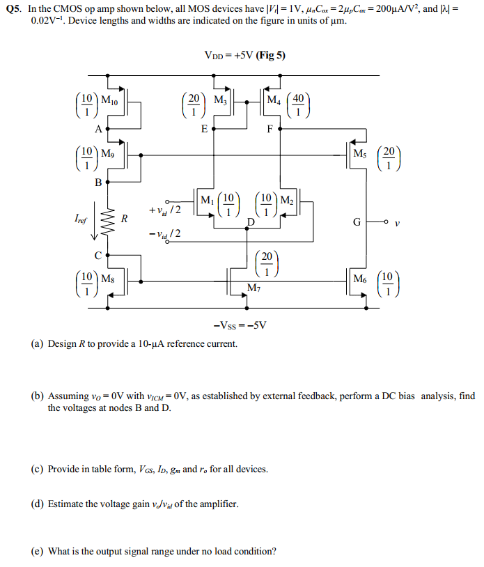
Q5. In the CMOS op amp shown below, all MOS devices have \( \left|V_{t}\right|=1 \mathrm{~V}, \mu_{n} C_{a x}=2 \mu_{p} C_{a x}=200 \mu \mathrm{~A} / \mathrm{V}^{2} \), and \( |\lambda|= \) \( 0.02 \mathrm{~V}^{-1} \). Device lengths and widths are indicated on the figure in units of \( \mu \mathrm{m} \).
\[
V_{D D}=+5 \mathrm{~V}(\mathbf{F i g} \mathbf{5})
\]
(a) Design \( R \) to provide a \( 10-\mu \mathrm{A} \) reference current.
(b) Assuming \( v_{O}=0 \mathrm{~V} \) with \( v_{I C M}=0 \mathrm{~V} \), as established by external feedback, perform a DC bias analysis, find the voltages at nodes B and D.
(c) Provide in table form, \( V_{G S}, I_{D}, g_{m} \) and \( r_{o} \) for all devices.
(d) Estimate the voltage gain \( v_{o} / v_{i d} \) of the amplifier.
(e) What is the output signal range under no load condition?