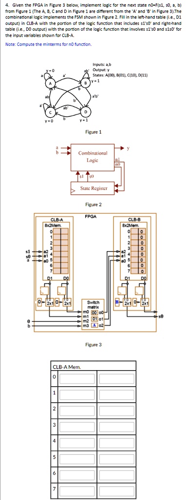
4. Given the FPGA in Figure 3 below, implement logic for the next state n0=F(s1, s0, a, b)
from Figure 1 (The A, B, C and D in Figure 1 are different from the 'A' and 'B' in Figure 3). The
combinational logic implements the FSM shown in Figure 2. Fill in the left-hand table (i.e., D1
output) in CLB-A with the portion of the logic function that includes s1's0' and right-hand
table (i.e., D0 output) with the portion of the logic function that involves s1s0 and s1s0' for
the input variables shown for CLB-A.
Note: Compute the minterms for n0 function.
Inputs: a,b
Output: y
States: A(00), B(01), C(10), D(11)
y = 1
Figure 1
Combinational
Logic
State Register
Figure 2
FPGA
CLB-B
8x2Mem.
0-2x10-2x1
Switch
matrix
m0 00 00
m1 01 01
m2
m3 A 02
s0
Figure 3
CLB-A Mem.
0
1
2
3
4
5
6
7