Work your assigned combinational logic simulation problem using the following procedure:
1. Generate the truth table of your combinational logic circuit using Multisim.
2. Write VHDL code that describes your combinational logic circuit.
3. Simulate and debug the VHDL code by using Vivado.
4. Print out a simulator listing that verifies the correct operation of your design for the prescribed test sequences.
5. Synthesize the code, and download it to the Basys3 FPGA board.
6. Test your circuit operation by using the board LEDs.
7. Record a video that shows the operation of your circuit in the Basys3 FPGA board.
View all sections below before proceeding to the next page, and refer back whenever necessary.
Problem 1 Problem 2
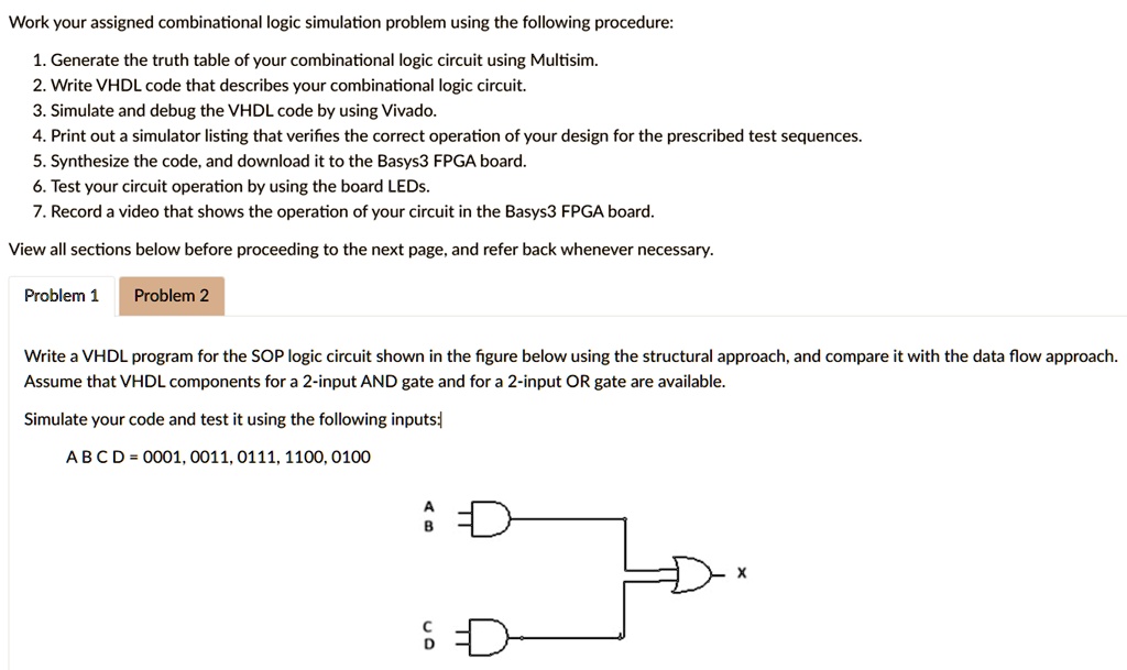
Write a VHDL program for the SOP logic circuit shown in the figure below using the structural approach, and compare it with the data flow approach. Assume that VHDL components for a 2-input AND gate and for a 2-input OR gate are available.
Simulate your code and test it using the following inputs:
A B C D = 0001, 0011, 0111, 1100, 0100