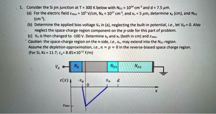
1. Consider the Si pn junction at T = 300 K below with $N_{D2} = 10^{14} cm^3$ and d = 7.5 µm.
(a) For the electric field $\mathcal{E}_{Max} = 10^5 V/cm$, $N_A = 10^{17} cm^3$, and $x_n = 5 \mu m$, determine $x_p$ (cm), and $N_{D1}$
$(cm^3)$.
(b) Determine the applied bias voltage $V_A$ in (a), neglecting the built-in potential, i.e., let $V_{bi} = 0$. Also
neglect the space-charge region component on the p-side for this part of problem.
(c) $V_A$ is then changed to -100 V. Determine $x_p$ and $x_n$ (both in cm) and $\mathcal{E}_{Max}$.
Caution: the space-charge region on the n-side, i.e., $x_n$, may extend into the $N_{D2}$ region.
Assume the depletion approximation, i.e., $n \approx p \approx 0$ in the reverse-biased space charge region.
(For Si, $K_s = 11.7$; $\epsilon_0 = 8.85 \times 10^{-12} F/m$)