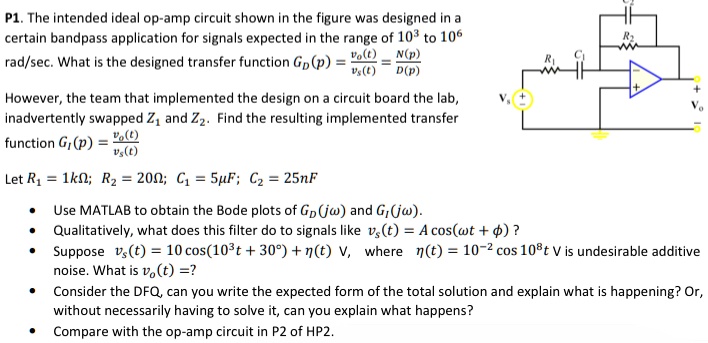
P1. The intended ideal op-amp circuit shown in the figure was designed in a
certain bandpass application for signals expected in the range of $10^3$ to $10^6$
rad/sec. What is the designed transfer function $G_D(p) = \frac{v_o(t)}{v_s(t)} = \frac{N(p)}{D(p)}$
However, the team that implemented the design on a circuit board the lab,
inadvertently swapped $Z_1$ and $Z_2$. Find the resulting implemented transfer
function $G_I(p) = \frac{v_o(t)}{v_s(t)}$
Let $R_1 = 1k\Omega$; $R_2 = 20\Omega$; $C_1 = 5\mu F$; $C_2 = 25nF$
* Use MATLAB to obtain the Bode plots of $G_D(j\omega)$ and $G_I(j\omega)$.
* Qualitatively, what does this filter do to signals like $v_s(t) = A \cos(\omega t + \phi)$ ?
* Suppose $v_s(t) = 10 \cos(10^3 t + 30^\circ) + \eta(t)$ V, where $\eta(t) = 10^{-2} \cos 10^8 t$ V is undesirable additive
noise. What is $v_o(t) =?$
* Consider the DFQ, can you write the expected form of the total solution and explain what is happening? Or,
without necessarily having to solve it, can you explain what happens?
* Compare with the op-amp circuit in P2 of HP2.