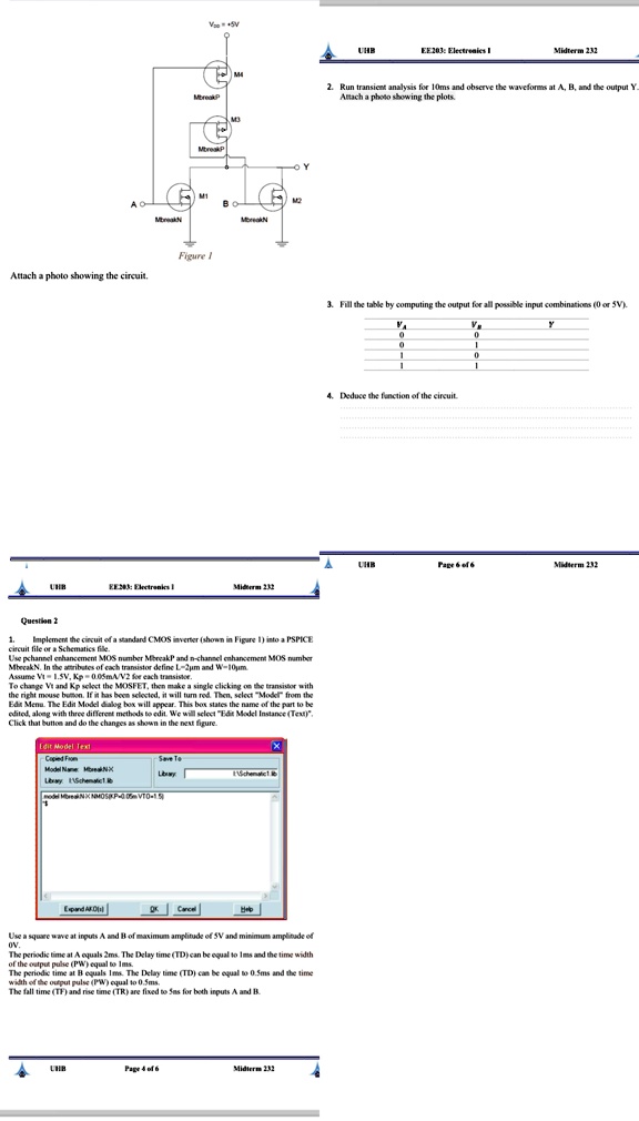
$V_{DD} = +5V$
MbreakP
MbreakP
MbreakN
MbreakN
Figure 1
Attach a photo showing the circuit.
Question 2
UHB
EE203: Electronics I
Midterm 232
2. Run transient analysis for 10ms and observe the waveforms at A, B, and the output Y
Attach a photo showing the plots.
3. Fill the table by computing the output for all possible input combinations (0 or 5V).
$V_A$ | $V_B$ | Y
------- | -------- | --------
0 | 0 |
0 | 1 |
1 | 0 |
1 | 1 |
Deduce function of the circuit..
UHB
Page 6 of 6
Midterm 232
EE203: Electronics I
Midterm 232
Implement the circuit of a standard CMOS inverter (shown in Figure 1) into a PSPICE
circuit file or a Schematics file.
Use pchannel enhancement MOS number MbreakP and n-channel enhancement MOS number
MbreakN. In the attributes of each transistor define L=2µm and W=10µm.
Assume Vt = 1.5V, Kp = 0.05mA/V2 for each transistor
To change Vt and Kp select the MOSFET, then make a single clicking on the transistor with
the right mouse button. If it has been selected, it will turn red. Then, select "Model" from the
Edit Menu. The Edit Model dialog box will appear. This box states the name of the part to be
edited, along with three different methods to edit. We will select "Edit Model Instance (Text)".
Click that button and do the changes as shown in the next figure.
Edit Model Text
Copied From
Model Name: MbreakNX
Library Schematic1.b
model MeaNX NMOSKP-005 VT0-1.5)
Schematic1.b
Expand All
OK Cancel
Help
Use a square wave at inputs A and B of maximum amplitude of 5V and minimum amplitude of
0V.
The periodic time at A equals 2ms. The Delay time (TD) can be equal to 1ms and the time width
of the output pulse (PW) equals 1ms.
The periodic time at B equals 1ms. The Delay time (TD) can be equal to 0.5ms and the time
width of the output pulse (PW) equal to 0.5ms.
The fall time (TF) and rise time (TR) are fixed to 5ns for both inputs A and B.
Page 4 of 6
Midterm 232