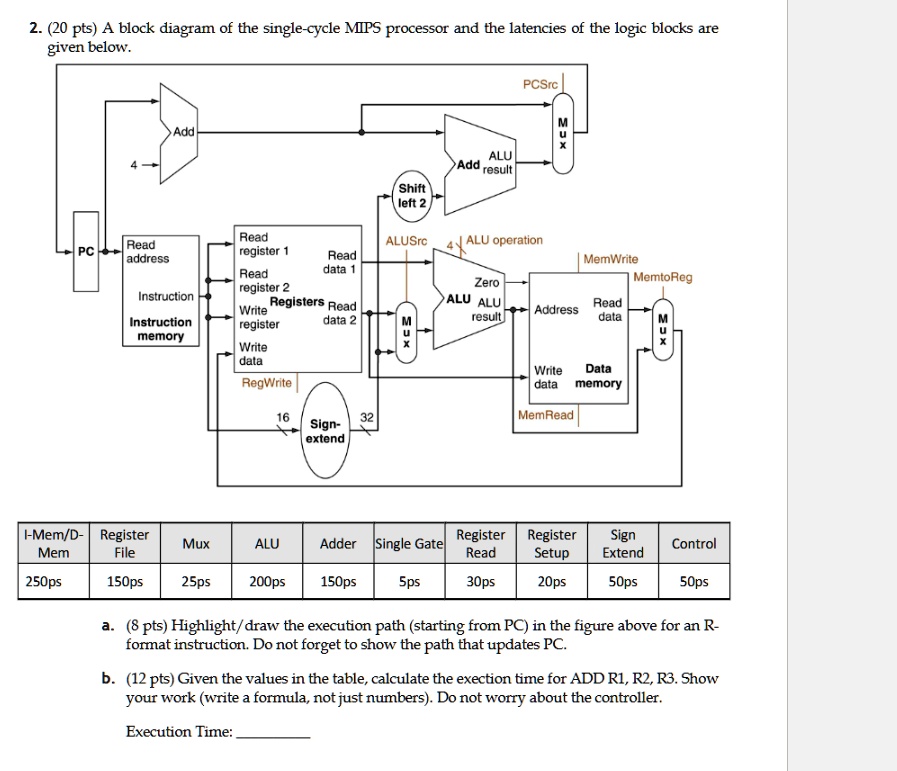
2. (20 pts) A block diagram of the single-cycle MIPS processor and the latencies of the logic blocks are given below.
4
Add
ALU
>Add result
Shift
left 2
PCSrc
M
Mux
Read
ALUSrc
PC
Read
address
4
ALU operation
register 1
Read
MemWrite
Read
data 1
register 2
Instruction
Instruction
memory
Registers Read
Write
register
data 2
M MUX
Zero
ALU ALU
Address
result
MemtoReg
Read
data
Mux
Write
data
RegWrite
Write Data
data memory
16
32
MemRead
Sign-
extend
I-Mem/D- Register
Mem
File
Mux
ALU
Adder Single Gate
Register Register
Read Setup
Sign
Extend
Control
250ps
150ps 25ps 200ps
150ps
5ps
30ps 20ps
50ps
50ps
a. (8 pts) Highlight/draw the execution path (starting from PC) in the figure above for an R-
format instruction. Do not forget to show the path that updates PC.
b. (12 pts) Given the values in the table, calculate the exection time for ADD R1, R2, R3. Show
your work (write a formula, not just numbers). Do not worry about the controller.
Execution Time: