Q2
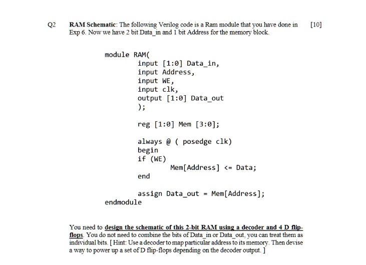
RAM Schematic: The following Verilog code is a Ram module that you have done in
Exp 6. Now we have 2 bit Data_in and 1 bit Address for the memory block.
[10]
module RAM(
input [1:0] Data_in,
input Address,
input WE,
input clk,
output [1:0] Data_out
);
reg [1:0] Mem [3:0];
always @ (posedge clk)
begin
if (WE)
end
Mem [Address] <= Data;
assign Data_out = Mem [Address];
endmodule
You need to design the schematic of this 2-bit RAM using a decoder and 4 D flip-
flops. You do not need to combine the bits of Data_in or Data_out, you can treat them as
individual bits. [Hint: Use a decoder to map particular address to its memory. Then devise
a way to power up a set of D flip-flops depending on the decoder output.]