Texts: Need help please. Could you please provide the drawing of load lines and values. Thank you.
Below is the circuit needed to calculate step 5. Question 1 does not need to be answered; it was only attached for the Vp and Idss values.
AIM
To become familiar with the biasing techniques for different FETs.
Notes
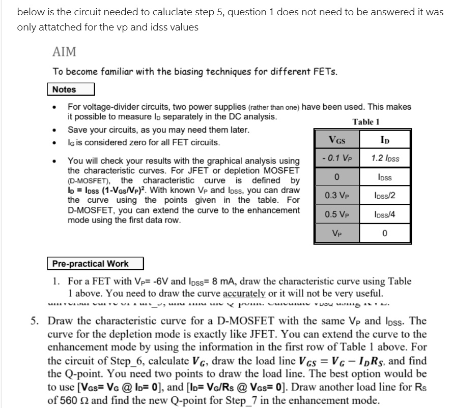
For voltage-divider circuits, two power supplies (rather than one) have been used. This makes it possible to measure Id separately in the DC analysis Table 1. Save your circuits, as you may need them later. Ig is considered zero for all FET circuits.
Vgs = Ip
You will check your results with the graphical analysis using -0.1Vp to 1.2Vp. The characteristic curves for JFET or depletion MOSFET (D-MOSFET) are defined by Ioss = Ipss(1 - Vgs/Vp)^2. With known Vp and Ipss, you can draw the curve using the points given in the table.
For D-MOSFET, you can extend the curve to the enhancement mode using the first data row.
Vp = 0
Pre-practical Work
1. For a FET with Vp = -6V and Idss = 8 mA, draw the characteristic curve using Table 1 above. You need to draw the curve accurately or it will not be very useful.
5. Draw the characteristic curve for a D-MOSFET with the same Vp and Ipss. The curve for the depletion mode is exactly like JFET. You can extend the curve to the enhancement mode by using the information in the first row of Table 1 above.
For the circuit of Step 6, calculate V, draw the load line Vcs = V - IpRs, and find the Q-point. You need two points to draw the load line. The best option would be to use [Vgs = Vg @ Ip = 0], and [Ip = Vc/Rs @ Vgs = 0]. Draw another load line for Rs of 560 and find the new Q-point for Step 7 in the enhancement mode.