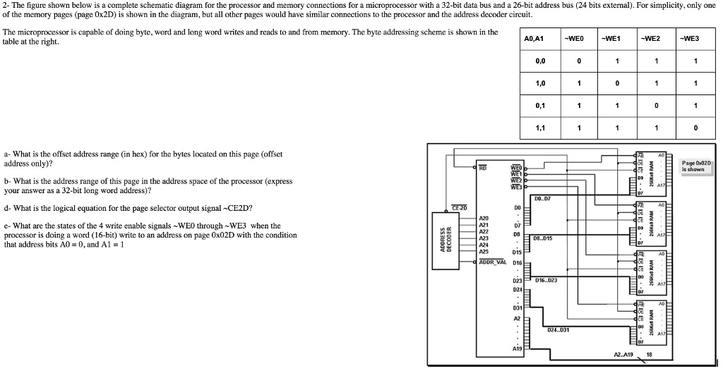
2- The figure shown below is a complete schematic diagram for the processor and memory connections for a microprocessor with a 32-bit data bus and a 26-bit address bus (24 bits external). For simplicity, only one
of the memory pages (page 0x2D) is shown in the diagram, but all other pages would have similar connections to the processor and the address decoder circuit.
The microprocessor is capable of doing byte, word and long word writes and reads to and from memory. The byte addressing scheme is shown in the
table at the right.
A0,A1
-WE0
-WE1
-WE2
-WE3
0,0
0
1
1
1
1,0
1
0
1
1
0,1
1
1
0
1
1,1
1
1
1
0
a- What is the offset address range (in hex) for the bytes located on this page (offset
address only)?
b- What is the address range of this page in the address space of the processor (express
your answer as a 32-bit long word address)?
d- What is the logical equation for the page selector output signal ~CE2D?
e- What are the states of the 4 write enable signals ~WE0 through ~WE3 when the
processor is doing a word (16-bit) write to an address on page 0x02D with the condition
that address bits A0 = 0, and A1 = 1