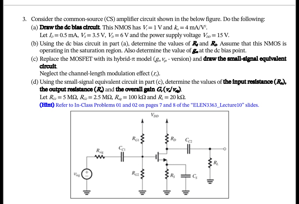
3. Consider the common-source (CS) amplifier circuit shown in the below figure. Do the following:
(a) Draw the dc bias circuit. This NMOS has $V_t = 1 V$ and $k_n = 4 mA/V^2$.
Let $I_D = 0.5 mA$, $V_{GS} = 3.5 V$, $V_D = 6 V$ and the power supply voltage $V_{DD} = 15 V$.
(b) Using the dc bias circuit in part (a), determine the values of $R_S$ and $R_D$. Assume that this NMOS is
operating in the saturation region. Also determine the value of $g_m$ at the dc bias point.
(c) Replace the MOSFET with its hybrid-$\pi$ model ($g_m V_{gs}$ - version) and draw the small-signal equivalent
circuit.
Neglect the channel-length modulation effect ($r_o$).
(d) Using the small-signal equivalent circuit in part (c), determine the values of the input resistance ($R_i$),
the output resistance ($R_o$) and the overall gain $G_v (v_d/v_{sig})$.
Let $R_{G1} = 5 M\Omega$, $R_{G2} = 2.5 M\Omega$, $R_{sig} = 100 k\Omega$ and $R_L = 20 k\Omega$.