Transistor
WIL
Q1
Q2
Q3
Q4
Q5
Q6
Q7
Q8
30/0.5
30/0.5
10/0.5
10/0.5
60/0.5
W/0.5
60/0.5
60/0.5
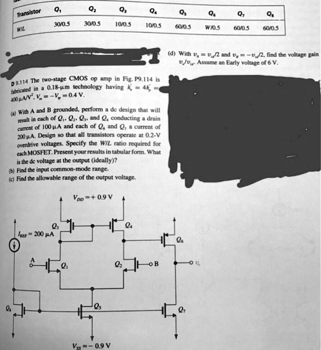
D9.114 The two-stage CMOS op amp in Fig. P9.114 is
fabricated in a 0.18-µm technology having $k_n = 4k_p =$
400 µA/V$^2$, $V_A = -V_A = 0.4$ V.
(a) With A and B grounded, perform a dc design that will
result in each of Q1, Q2, Q3, and Q4 conducting a drain
current of 100 µA and each of Q5 and Q7 a current of
200 µA. Design so that all transistors operate at 0.2-V
overdrive voltages. Specify the W/L ratio required for
each MOSFET. Present your results in tabular form. What
is the dc voltage at the output (ideally)?
(b) Find the input common-mode range.
(c) Find the allowable range of the output voltage.
$I_{REF} = 200\,\mu A$
$V_{DD} = +0.9\,\text{V}$
(d) With $v_i = v_{i2}/2$ and $v_i = -v_{i2}/2$, find the voltage gain
$v_o/v_{i2}$. Assume an Early voltage of 6 V.