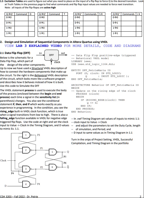
at Truth Tables in the previous page to find what commands and flip flop input values are needed to force the next transition. Note: all inputs of the flip-flops are active high.
Look
Q>Q* Command 0>0
Q>Q* Command 00
Commands
00
Commands
0>0
0<0
01
0->1
0->1
0->1
10
10
1>0
1->0
11
11
1>1
1->1
Design and Simulation of Sequential Components in Altera Quartus using VHDL VIEW LAB 3 EXPLAINED VIDEO FOR MORE DETAILS, CODE AND DIAGRAMS
2.1 Data Flip Flop (DFF) in out DFF Data Flip Flop positive-edge triggered Below is the schematic for a Behavioral VHDL model Data Flip Flop, which is part of clock LIBRARY ieee; the design of the other components. USE ieee.std logic ii64.ALL, Up to now we have used a Structural VHDL description of ENTITY DFF_PetrieMaria IS how to connect the hardware components that make up PORT (D, clock: IN STD_LOGIC; the circuit. To the right is the Behavioral VHDL description