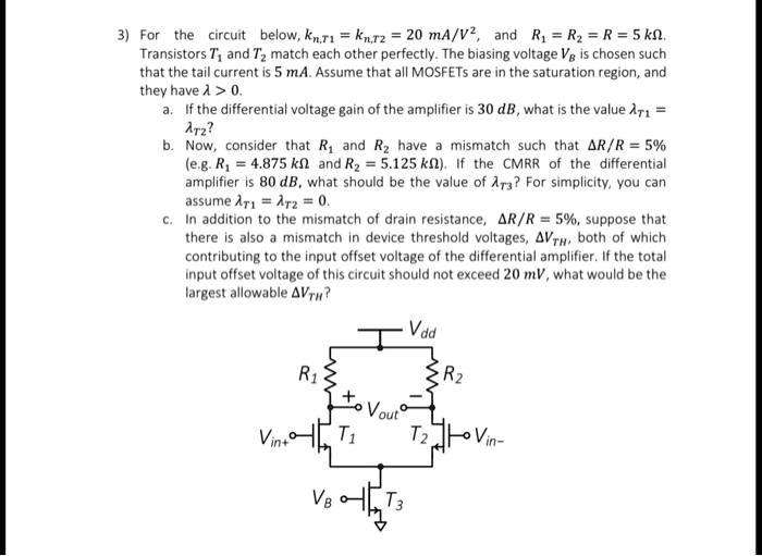
3) For the circuit below, $k_{n,T1} = k_{n,T2} = 20 mA/V^2$, and $R_1 = R_2 = R = 5 k\Omega$.
Transistors $T_1$ and $T_2$ match each other perfectly. The biasing voltage $V_B$ is chosen such
that the tail current is 5 mA. Assume that all MOSFETs are in the saturation region, and
they have $\lambda > 0$.
a. If the differential voltage gain of the amplifier is 30 dB, what is the value $\lambda_{T1} =$
$\lambda_{T2}$?
b. Now, consider that $R_1$ and $R_2$ have a mismatch such that $\Delta R/R = 5%$
(e.g. $R_1 = 4.875 k\Omega$ and $R_2 = 5.125 k\Omega$). If the CMRR of the differential
amplifier is 80 dB, what should be the value of $\lambda_{T3}$? For simplicity, you can
assume $\lambda_{T1} = \lambda_{T2} = 0$.
c. In addition to the mismatch of drain resistance, $\Delta R/R = 5\%$, suppose that
there is also a mismatch in device threshold voltages, $\Delta V_{TH}$, both of which
contributing to the input offset voltage of the differential amplifier. If the total
input offset voltage of this circuit should not exceed 20 mV, what would be the
largest allowable $\Delta V_{TH}$?