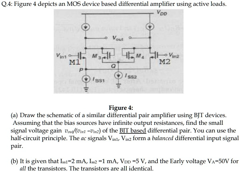
Q.4: Figure 4 depicts an MOS device based differential amplifier using active loads.
VDD
Vout
Vin1 M3 M4 Vin2
M2
M1
P
SS1
Q
SS2
Figure 4:
(a) Draw the schematic of a similar differential pair amplifier using BJT devices.
Assuming that the bias sources have infinite output resistances, find the small
signal voltage gain $V_{out}/(V_{in1} -V_{in2})$ of the BJT based differential pair. You can use the
half-circuit principle. The ac signals $V_{in1}$, $V_{in2}$ form a balanced differential input signal
pair.
(b) It is given that $I_{SS1}$=2 mA, $I_{SS2}$ =1 mA, $V_{DD}$ =5 V, and the Early voltage $V_A$=50V for
all the transistors. The transistors are all identical.