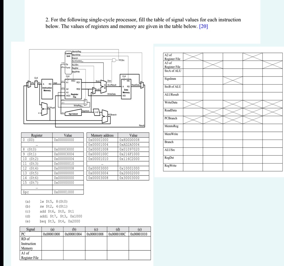
2. For the following single-cycle processor, fill the table of signal values for each instruction
below. The values of registers and memory are given in the table below. [20]
MemtoReg
MemWrite
Branch
ALUControl
PCSrc
ALUSro
Funct RegDst
RegWrite
CLK
CLK
WE3
RD1
ALUResult
RD2
WD3 Regi
Register
WD
A2 of
Register File
A3 of
Register File
SrcA of ALU
SignImm
SrcB of ALU
ALUResult
WriteData
CLK
RD
A2
A3
ReadData
Sign Extend
PCBranch
PCBranch
MemtoReg
Register
Value
Memory address
Value
MemWrite
0 ($0)
0x00000000
0x00001000
0x8D0D0008
Branch
0x00001004
0xAD2A0004
8 ($t0)
0x00003000
0x00001008
0x01097020
ALUSre
9 ($t1)
0x00003004
0x0000100C
0x216F1000
10 ($t2)
0x00000004
0x00001010
0x116C2000
RegDst
11 ($t3)
0x00000010
RegWrite
12 ($t4)
0x00000008
0x00003000
0x10001000
13
($t5)
0x00000000
0x00003004
0x20002000
14 ($t6)
0x00000000
0x00003008
0x30003000
15 ($t7)
0x00000000
$pc
0x00001000
(a)
lw $t5, 8($t0)
(b)
sw $t2, 4($t1)
(c)
add $t6, $t0, $t1
(d)
addi $t7, $t3, 0x1000
(e)
beq $t3, $t4, 0x2000
Signal
(a)
(b)
(c)
(d)
(e)
PC
0x00001000 0x00001004 0x00001008
0x0000100C 0x00001010
RD of
Instruction
Memory
Al of
Register File