Goal
You are tasked with designing an opamp which takes in two inputs and gives a single-ended output. The opamp is
supposed to drive a load capacitor $C_L$.
• Call the input common-mode as $V_{ICM}$ (measured in open-loop). The condition on $V_{ICM}$ is given in Table-I.
• When in unity feedback, the output (which is equal to the input) should be able to swing at least 0.8 V, i.e., the
difference between the maximum and the minimum voltage when in unity feedback must be greater than 0.8 V.
• When put in unity feedback, while driving $C_L$, the closed-loop 3-dB bandwidth must be $\ge f_B$. Value of $C_L$ and $f_B$
given in Table-I.
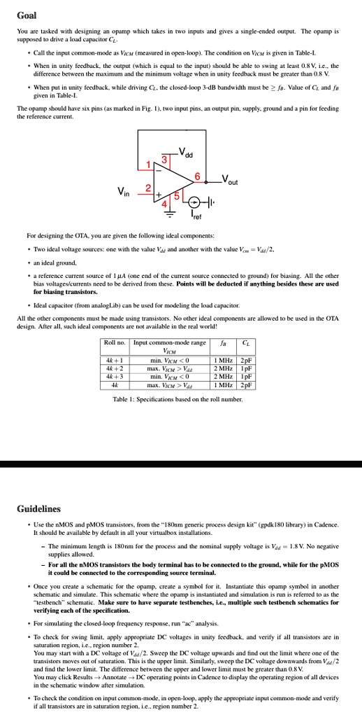
The opamp should have six pins (as marked in Fig. 1), two input pins, an output pin, supply, ground and a pin for feeding
the reference current.
For designing the OTA, you are given the following ideal components:
• Two ideal voltage sources: one with the value $V_{dd}$ and another with the value $V_{cm} = V_{dd}/2$.
• an ideal ground.
• a reference current source of 1 $\mu$A (one end of the current source connected to ground) for biasing. All the other
bias voltages/currents need to be derived from these. Points will be deducted if anything besides these are used
for biasing transistors.
• Ideal capacitor (from analogLib) can be used for modeling the load capacitor.
All the other components must be made using transistors. No other ideal components are allowed to be used in the OTA
design. After all, such ideal components are not available in the real world!
Table 1: Specifications based on the roll number
Guidelines
• Use the nMOS and pMOS transistors, from the "180nm generic process design kit" (gpdk180 library) in Cadence.
It should be available by default in all your virtualbox installations.
– The minimum length is 180nm for the process and the nominal supply voltage is $V_{dd} = 1.8$ V. No negative
supplies allowed.
– For all the nMOS transistors the body terminal has to be connected to the ground, while for the pMOS
it could be connected to the corresponding source terminal.
• Once you create a schematic for the opamp, create a symbol for it. Instantiate this opamp symbol in another
schematic and simulate. This schematic where the opamp is instantiated and simulation is run is referred to as the
"testbench" schematic. Make sure to have separate testbenches, i.e., multiple such testbench schematics for
verifying each of the specification.
• For simulating the closed-loop frequency response, run "ac" analysis.
• To check for swing limit, apply appropriate DC voltages in unity feedback, and verify if all transistors are in
saturation region, i.e., region number 2.
You may start with a DC voltage of $V_{dd}/2$. Sweep the DC voltage upwards and find out the limit where one of the
transistors moves out of saturation. This is the upper limit. Similarly, sweep the DC voltage downwards from $V_{dd}/2$
and find the lower limit. The difference between the upper and lower limit must be greater than 0.8 V.
You may click Results $\rightarrow$ Annotate $\rightarrow$ DC operating points in Cadence to display the operating region of all devices
in the schematic window after simulation.
• To check the condition on input common-mode, in open-loop, apply the appropriate input common-mode and verify
if all transistors are in saturation region, i.e., region number 2.