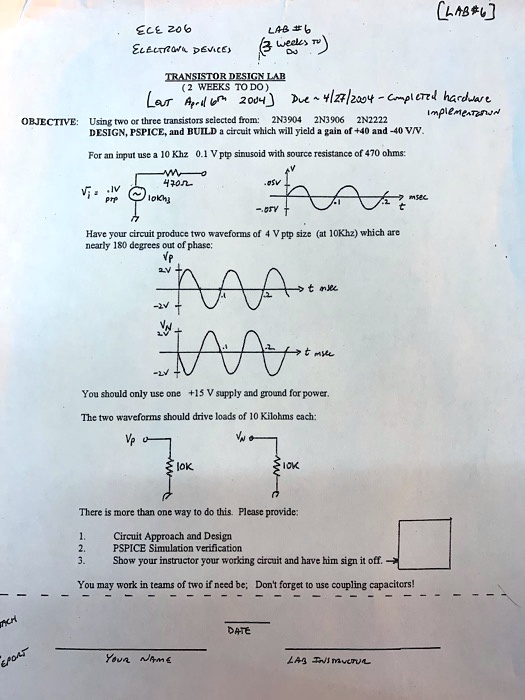
LAB #C
ECE 206 ELECTRONIC DEVICES
Lab 3: Transistor Design
Lab 2: Weeks to Do
TA 2004 Due: 4/27/24 - Completed Hardware Implementation
OBJECTIVE
Using two or three transistors selected from 2N3904, 2N3906, 2N2222, design, simulate using PSPICE, and build a circuit which will yield a gain of +40 and -40 V/V.
For the input, use a 10 kHz 0.1 V peak-to-peak sinusoid with a source resistance of 470 ohms.
Have your circuit produce two waveforms of 4 V peak-to-peak size (at 10 kHz) which are nearly 180 degrees out of phase: Vp.
You should only use one +15 V supply and ground for power.
The two waveforms should drive loads of 10 kilohms each: Vp, Vout.
There is more than one way to do this. Please provide a circuit approach and design, PSPICE simulation verification. Show your instructor your working circuit and have him sign it off.