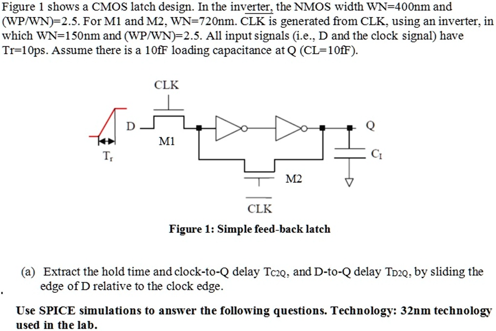
Figure 1 shows a CMOS latch design. In the inverter, the NMOS width WN=400nm and (WP/WN)=2.5. For M1 and M2, WN=720nm. CLK is generated from CLK, using an inverter, in which WN=150nm and (WP/WN)=2.5. All input signals (i.e., D and the clock signal) have Tr=10ps. Assume there is a 10fF loading capacitance at Q (CL=10fF).
(a) Extract the hold time and clock-to-Q delay $T_{c2q}$, and D-to-Q delay $T_{D2Q}$, by sliding the edge of D relative to the clock edge.
Use SPICE simulations to answer the following questions. Technology: 32nm technology used in the lab.