For the following three questions, you will be designing a memory subsystem for a computer with an 8-bit data bus and a 16-bit address bus. The memory subsystem consists of a combination of ROM and RAM, implemented either as individual memory chips or as arrays of memory chips, with each type of memory occupying a portion of the available 64K address space. Your partial address decoding logic must ensure that these chips are active only within the range of addresses described below.
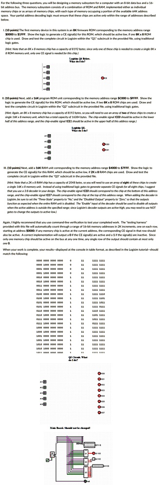
I. (10 points) The first memory device in this system is an 8K firmware ROM corresponding to the memory address range **$6000$ to $SFFF$**. Show the logic to generate a CE signal(s) for this ROM, which should be active low. If one 8 x 8 ROM chip is used. Draw and test the complete circuit in Logisim within the "Q1" subcircuit in the provided file, using traditional logic gates.
(Hint: Note that an 8 x 8 memory chip has a capacity of 6192 bytes; since only one of these chip is needed to create a single 8 x 8 ROM memory unit, only one CE signal is needed for this chip.)
Logisim Q1 Below. What do I do?
II. (10 points) Next, add a 16K program ROM unit corresponding to the memory address range **$C000$ to $SFFF$**. Show the logic to generate the CE signal(s) for this ROM, which should be active low, if two 8 x 8 ROM chips are used. Draw and test the complete circuit in Logisim within the "Q2" subcircuit in the provided file, using traditional logic gates.
(Hint: Again, an 8 x 8 memory chip has a capacity of 6192 bytes, so you will need to use an array of **two** of these chips to create a single 16K x 8 memory unit. Instead of using traditional logic gates to generate separate CE signals for all eight chips, I suggest that you use a 3-8 decoder in your design. The chip-enable signal **ICE** should correspond to the chip at the bottom of this address range, and the chip-enable signal **ICE1** should correspond to the chip at the top of this address range. When adding the decoder in Logisim, be sure to set the "Three-State" property to "No" and the "Doubled Output" property to "Zero" so that the outputs function as expected when the entire RAM unit is disabled. The "Enable" input of the decoder should be used to disable all outputs when the active address is outside the specified range. Since Logisim's decoder outputs are active-high, you may need to use NOT gates to change the outputs to active-low.)
III. (10 points) Next, add a 16K RAM unit corresponding to the memory address range **$4000$ to $SFFF$**. Show the logic to generate the CE signal(s) for this RAM, which should be active low, if 2K x 8 RAM chips are used. Draw and test the complete circuit in Logisim within the "Q3" subcircuit in the provided file.
(Hint: Note that a 2K x 8 RAM chip has a capacity of 2048 bytes, so you will need to use an array of **eight** of these chips to create a single 16K x 8 memory unit. Instead of using traditional logic gates to generate separate CE signals for all eight chips, I suggest that you use a 3-8 decoder in your design. The chip-enable signal **ICE** should correspond to the chip at the bottom of this address range, and the chip-enable signal **ICE7** should correspond to the chip at the top of this address range. When adding the decoder in Logisim, be sure to set the "Three-State" property to "No" and the "Doubled Output" property to "Zero" so that the outputs function as expected when the entire RAM unit is disabled. The "Enable" input of the decoder should be used to disable all outputs when the active address is outside the specified range. Since Logisim's decoder outputs are active-high, you may need to use NOT gates to change the outputs to active-low.)
Again, I highly recommend that you use command-line verification to test your completed work. The "testing harness" provided with this file will automatically count through a range of 16-bit memory addresses in 2K increments, one on each row, also at address **$0000$**. If any memory chip is active at the current address, the corresponding CE signal(s) are inactive. Since starting at address **$0000$**, implementation will output a 0 if the CE signal(s) are active and a 1 if the CE signal in that row should only be one memory chip should be active on the bus at any one time, any single row of the output should contain at most only one 0.
When your work is complete, your results - displayed at the console in table format, as described in the Logisim tutorial - should match the following
0000 0000 0000 0000 0 11 1111 1111
0000 1000 0000 0000 0 11 1111 1111
0001 0000 0000 0000 0 11 1111 1111
0001 1000 0000 0000 0 11 1111 1111
0010 0000 0000 0000 1 11 1111 1111
0010 1000 0000 0000 1 11 1111 1111
0011 0000 0000 0000 1 11 1111 1111
0011 1000 0000 0000 1 11 1111 1110
0100 0000 0000 0000 1 11 1111 1101
0100 1000 0000 0000 1 11 1111 1100
0101 0000 0000 0000 1 11 1111 1011
0101 1000 0000 0000 1 11 1111 1010
0110 0000 0000 0000 1 11 1111 1001
0110 1000 0000 0000 1 11 1111 1000
0111 0000 0000 0000 1 11 1011 1111
0111 1000 0000 0000 1 11 0111 1111
1000 0000 0000 0000 1 11 1111 1111
1000 1000 0000 0000 1 11 1111 1111
1001 0000 0000 0000 1 11 1111 1111
1001 1000 0000 0000 1 11 1111 1111
1010 0000 0000 0000 1 11 1111 1111
1010 1000 0000 0000 1 11 1111 1111
1011 0000 0000 0000 1 11 1111 1111
1011 1000 0000 0000 1 11 1110 1111
1100 0000 0000 0000 1 11 1111 1111
1100 1000 0000 0000 1 11 1111 1111
1101 0000 0000 0000 1 11 1111 1111
1101 1000 0000 0000 1 11 1111 1111
1110 0000 0000 0000 1 11 1111 1111
1110 1000 0000 0000 1 11 1111 1111
1111 0000 0000 0000 1 11 1111 1111
1111 1000 0000 0000 1 11 1111 1111
Q1 Circuit. What do I do?
Main Board. Should not be changed!