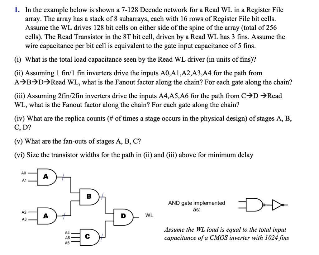
1. In the example below is shown a 7-128 Decode network for a Read WL in a Register File array. The array has a stack of 8 subarrays, each with 16 rows of Register File bit cells. Assume the WL drives 128 bit cells on either side of the spine of the array (total of 256 cells). The Read Transistor in the 8T bit cell, driven by a Read WL has 3 fins. Assume the
(i) What is the total load capacitance seen by the Read WL driver (in units of fins)?
(ii) Assuming 1 fin/1 fin inverters drive the inputs A0,A1,A2,A3,A4 for the path from A->B->D->Read WL, what is the Fanout factor along the chain? For each gate along the chain?
(iii) Assuming 2fin/2fin inverters drive the inputs A4,A5,A6 for the path from C->D ->Read WL, what is the Fanout factor along the chain? For each gate along the chain?
(iv) What are the replica counts (# of times a stage occurs in the physical design) of stages A, B C,D?
(v) What are the fan-outs of stages A, B, C?
(vi) Size the transistor widths for the path in (ii) and (iii) above for minimum delay
AO A1
AND gate implemented as:
A2
WL
A3
Assume the WL load is equal to the total input capacitance of a CMOS inverter with 1024 fins
A4 A5 A6