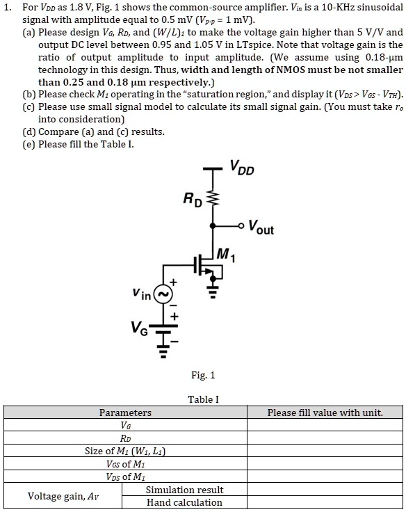
1. For VDD as 1.8 V, Fig. 1 shows the common-source amplifier. Vin is a 10-KHz sinusoidal signal with amplitude equal to 0.5 mV ($V_{p-p} = 1$ mV).
(a) Please design $V_G$, $R_D$, and $(W/L)_1$ to make the voltage gain higher than 5 V/V and output DC level between 0.95 and 1.05 V in LTspice. Note that voltage gain is the ratio of output amplitude to input amplitude. (We assume using 0.18-µm technology in this design. Thus, width and length of NMOS must be not smaller than 0.25 and 0.18 µm respectively.)
(b) Please check $M_1$ operating in the \"saturation region\", and display it ($V_{DS} > V_{GS} - V_{TH}$).
(c) Please use small signal model to calculate its small signal gain. (You must take $r_o$ into consideration)
(d) Compare (a) and (c) results.
(e) Please fill the Table I.
$V_{DD}$
$R_D$
$V_{out}$
$M_1$
$+$
$V_{in}$
$V_G$
$+$
Fig. 1
Table I
Parameters
Please fill value with unit.
$V_G$
$R_D$
Size of $M_1$ ($W_1$, $L_1$)
$V_{GS}$ of $M_1$
$V_{DS}$ of $M_1$
Simulation result
Voltage gain, $A_v$
Hand calculation