Purpose:
Experiment 9: Multiplier Design Using Multiplexers
The purpose of this experiment is to design and implement a circuit that will multiply two 2-bit binary numbers
using Multiplexers and logic gates.
Prelab:
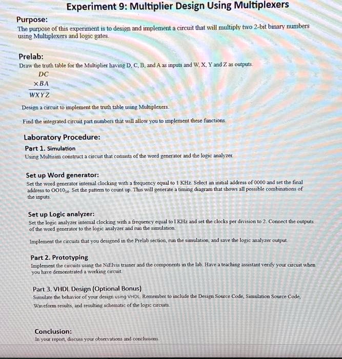
Draw the truth table for the Multiplier having D, C, B, and A as inputs and W, X, Y and Z as outputs.
DC
XBA
WXYZ
Design a circuit to implement the truth table using Multiplexers.
Find the integrated circuit part numbers that will allow you to implement these functions.
Laboratory Procedure:
Part 1. Simulation
Using Multisim construct a circuit that consists of the word generator and the logic analyzer
Set up Word generator:
Set the word generator internal clocking with a frequency equal to 1 KHz. Select an initial address of 0000 and set the final
address to 0010$_{16}$. Set the pattern to count up. This will generate a timing diagram that shows all possible combinations of
the inputs.
Set up Logic analyzer:
Set the logic analyzer internal clocking with a frequency equal to 1 KHz and set the clocks per division to 2. Connect the outputs
of the word generator to the logic analyzer and run the simulation
Implement the circuits that you designed in the Prelab section, run the simulation, and save the logic analyzer output.
Part 2. Prototyping
Implement the circuits using the NiElvis trainer and the components in the lab. Have a teaching assistant verify your circuit when
you have demonstrated a working circuit
Part 3. VHDL Design (Optional Bonus)
Simulate the behavior of your design using VHDL. Remember to include the Design Source Code, Simulation Source Code,
Waveform results, and resulting schematic of the logic circuits.
Conclusion:
In your report, discuss your observations and conclusions.