Part 1. Open-Loop Transimpedance Amplifier
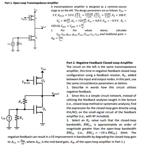
A transimpedance amplifier is designed as a common-source stage as shown on the left. The design parameters are as follows: Vpo = 40mV, k = 120μA/V^2, Ven = 0.8V, Vp = 0.9V, R = 1kΩ.
1. For the values above, calculate Ip, Ipm1, gm2, Vov1, Vov2, rro2, and midband gain (A).
Part 2. Negative-Feedback Closed-Loop Amplifier
The circuit on the left is the same transimpedance amplifier, this time in a negative-feedback closed-loop configuration using a feedback resistor, Rp, added between the input and output nodes. In this part, use the same circuit/device parameters as before.
1. Describe in words how this circuit utilizes negative feedback.
2. Since this is a simple circuit network, instead of utilizing the feedback analyses taught in the lecture (i.e., closed-loop method or systematic analysis), find the expression for the closed-loop gain directly using KVL/KCL on the small-signal circuit of the feedback amplifier (i.e., with RF included).
3. Select an Rp value such that the closed-loop bandwidth, BWc, is approximately an order of magnitude greater than the open-loop bandwidth BWoL (i.e., BWc = 10 x BWoL). (Hint: The negative feedback can result in a x10 improvement in bandwidth by degrading the closed-loop gain by 10.)