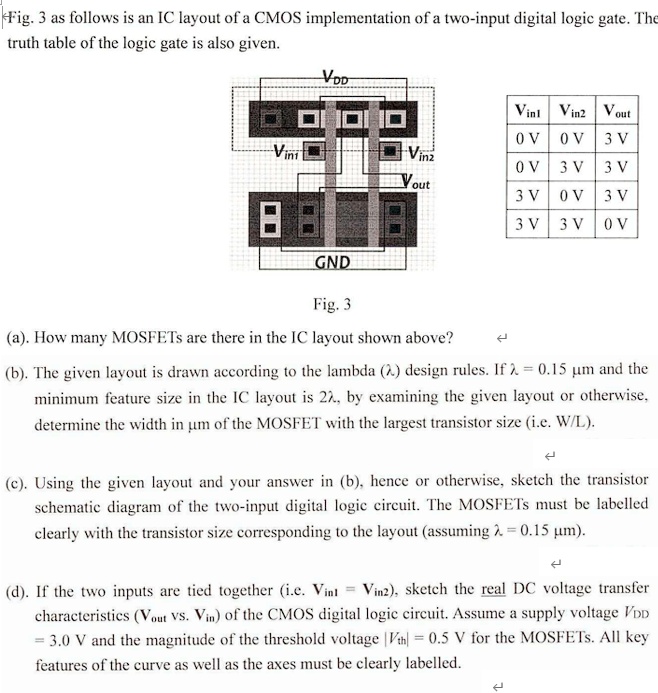
Fig. 3 as follows is an IC layout of a CMOS implementation of a two-input digital logic gate. The truth table of the logic gate is also given.
VDD
Vini
Vinz
Vout
8
GND
Fig. 3
Vint Vin2 Vout
0V 0V 3V
0V 3V 3 V
3V 0V 3V
3V 3V 0V
(a). How many MOSFETs are there in the IC layout shown above?
(b). The given layout is drawn according to the lambda ($\lambda$) design rules. If $\lambda$ = 0.15 µm and the minimum feature size in the IC layout is 2$\lambda$, by examining the given layout or otherwise, determine the width in µm of the MOSFET with the largest transistor size (i.e. W/L).
(c). Using the given layout and your answer in (b), hence or otherwise, sketch the transistor schematic diagram of the two-input digital logic circuit. The MOSFETs must be labelled clearly with the transistor size corresponding to the layout (assuming $\lambda$ = 0.15 µm).
(d). If the two inputs are tied together (i.e. $V_{int} = V_{in2}$), sketch the real DC voltage transfer characteristics ($V_{out}$ vs. $V_{in}$) of the CMOS digital logic circuit. Assume a supply voltage $V_{DD}$ = 3.0 V and the magnitude of the threshold voltage $|V_{th}|$ = 0.5 V for the MOSFETs. All key features of the curve as well as the axes must be clearly labelled.