EET 316
Digital Design
LAB 10
Design and Implementation of the Fibonacci Series using VHDL
Lab Summary
This lab teaches VHDL design entry, and prototyping using Xilinx ISE® tools and Digilent
ADEPT software. You will learn how a Fibonacci Series sequence generation can be directly
entered into Xilinx ISE® and implemented on a XILINX FPGA-based board and then write a
Test bench Simulation.
Learning Objectives
1. Use the Xilinx ISE® VHDL Editor to create a 1Hz Clock Divider project and then add
a second VHDL process for the design of the Fibonacci Series.
2. Using the 1Hz clock design as the clock to sequentially increment the Fibonacci Series
3. Implement the design on Nexys 3 platform, using Digilent ADEPT software.
Required Software
• Xilinx ISE Software - installed on your lab computers
• Digilent ADEPT suite - installed on your lab computers
Required Hardware
• Digilent NEXYS 3 boards and USB cable
Lab Preparation, Procedure and Lab Report
Read this document completely before you start on this experiment.
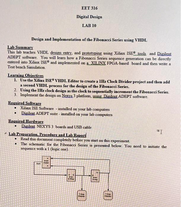
The schematic for the Fibonacci Series is presented below. You need to initiate the
sequence with a 1 (logic one).
Sum
Adder
D-Reg
7-Seg
Display
D-Reg
7-Seg
Display