D
C
B
Input pulses
10000
rese
The JK flip-flop behavior is the following:
module JK_FF (J,K,CLK,Q);
output Q;
input J,K,CLK;
reg Q;
always @ (posedge CLK)
case ({J,K})
2'b00: Q = Q;
2'b01: Q = 1'b0;
2'b10: Q = 1'b1;
2'b11: Q = ~Q; //TTL 2'b11 if inputs are impeded
endcase
endmodule
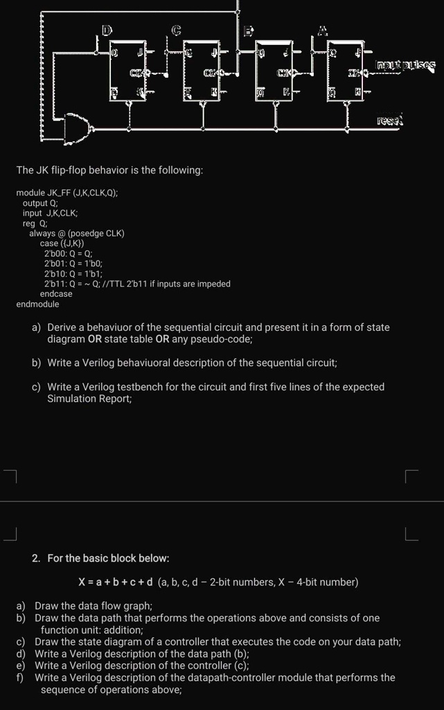
a) Derive a behaviuor of the sequential circuit and present it in a form of state
diagram OR state table OR any pseudo-code;
b) Write a Verilog behaviuoral description of the sequential circuit;
c) Write a Verilog testbench for the circuit and first five lines of the expected
Simulation Report;
2. For the basic block below:
X=a+b+c+d (a, b, c, d - 2-bit numbers, X - 4-bit number)
a) Draw the data flow graph;
b) Draw the data path that performs the operations above and consists of one
function unit: addition;
c) Draw the state diagram of a controller that executes the code on your data path;
d) Write a Verilog description of the data path (b);
e) Write a Verilog description of the controller (c);
f) Write a Verilog description of the datapath-controller module that performs the
sequence of operations above;