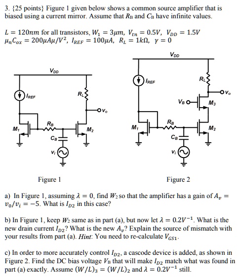
3. {25 points) Figure 1 given below shows a common source amplifier that is
biased using a current mirror. Assume that $R_B$ and $C_B$ have infinite values.
$L = 120nm$ for all transistors, $W_1 = 3\mu m$, $V_{tn} = 0.5V$, $V_{DD} = 1.5V$
$\mu_n C_{ox} = 200\mu A/V^2$, $I_{REF} = 100\mu A$, $R_L = 1k\Omega$, $\gamma = 0$
$V_{DD}$
$I_{REF}$
$V_{DD}$
$R_L$
$I_{REF}$
$V_B \circ$
$M_3$
$V_o$
$R_B$
$M_1$
$M_2$
$C_B$
$V_i$
$R_B$
$M_1$
$M_2$
$C_B$
$V_i$
Figure 1
Figure 2
a) In Figure 1, assuming $\lambda = 0$, find $W_2$ so that the amplifier has a gain of $A_v =$
$v_o/v_i = -5$. What is $I_{D2}$ in this case?
b) In Figure 1, keep $W_2$ same as in part (a), but now let $\lambda = 0.2V^{-1}$. What is the
new drain current $I_{D2}$? What is the new $A_v$? Explain the source of mismatch with
your results from part (a). Hint: You need to re-calculate $V_{GS1}$.
c) In order to more accurately control $I_{D2}$, a cascode device is added, as shown in
Figure 2. Find the DC bias voltage $V_B$ that will make $I_{D2}$ match what was found in
part (a) exactly. Assume $(W/L)_3 = (W/L)_2$ and $\lambda = 0.2V^{-1}$ still.